Computer Systems Principle [1] - Registers, Address Modes
Warm-up Questions

Keypoint :
Address - Location of Data
Data - What exactly stored in address
Reference Point = 1st byte of the sequence
Logical address = relative distance from 1st byte
Logical address allow user to ignore memory (relocatable)
Physical address = Address
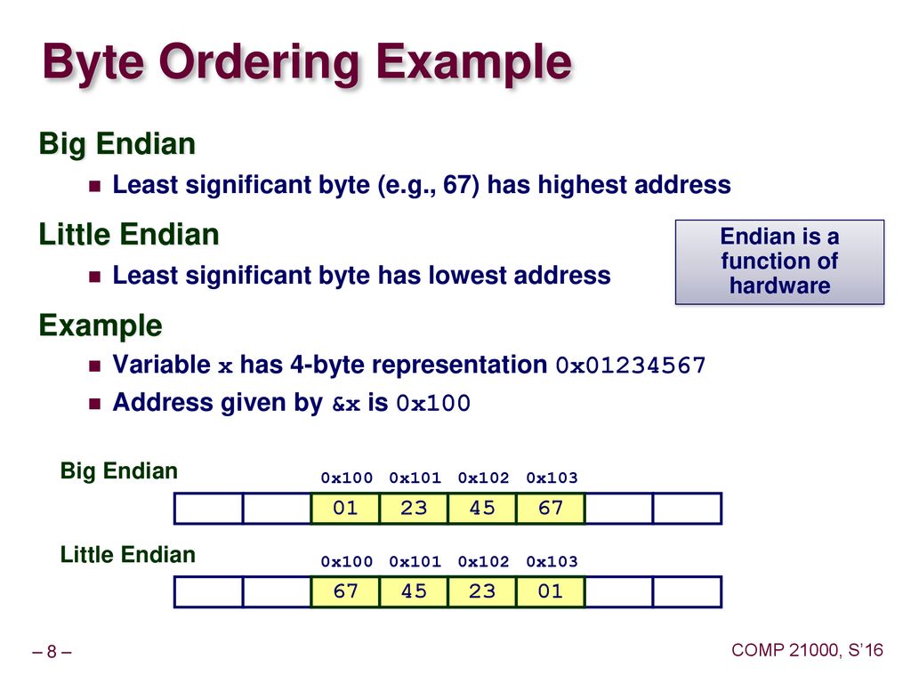
Little Endian and Big Endian
Most Significant Byte = Leftmost Byte in 0x
Least Significant Byte = Rightmost Byte in 0x
E.g. Data is 1234H, Because 12|34 , MSB = 12H, LSB = 34H
Now we have Address : 1000H and 1001H
In Little Endian format, LSB has lowest address.
12H -> 1001H
34H -> 1000H
Life cycle of Logical Address and Physical Address:
- Logical Address (Machine Code Exist)- A Relative Sequence. Elimated once the file/disk/partition is deleted.
- Have Machine Code = Logical Address
- Physical Address (In computer) - Different everytime when you run a program. Elimated once the program is ended, Short life cycle
- Program’s Hard Disk (Secondary Memory) -> Memory’s Card’s RAM (Primary Memory) = Have Physical Address
(a) Logical address at 5002H = 2
(b) Physical address at 5003H = 5003H
© Logical address of 5th byte = 4
(d) Physical address of 5th byte = 5004H
(e) N.A.
Note: If program is not being loaded into computer memory, there will be no physical address.
The answer is Nothing/ Dont Know.
(f)
Data A is composed of 2 bytes. We use little endian format here, Higher address has higher significant byte. 42H is LSB, 11H is MSB
Therefore Value of Data A : 11|42 -> 1142H
If we use Big endian format, the value of Data A will be 4211H.
(g)
Logical address will always have longing life cycle than physical address.
(h)
Provide address of least significant byte -> Lowest address -> 42H -> 5006H
Yes. 5006H is physical address.

Char/Int = 1 byte = 8 bit
Word = 2 byte = 16 bit
Doubleword = 4 byte = 32 bit
Quadword = 8 byte = 64 bit
:: = 2^n byte
Keypoints:
Signed = with sign bit
Unsigned = without sign bit (must be positive)
1’s complement: invert each bit of a number from 0 to 1 or from 1 to 0.
(a),(b),©,(d):
(e)
In theory, you can, but you won’t do it in practice. A computer is designed in a way that the starting address of a byte/word/doubleword/quadword must be integer multiples of 1/2/4/8 so as to reduce the hardware complexity. If you follow the rule, you can fetch the requested data in one single data transfer. When compiling your program, the complier automatically handles this for your program to produce machine codes under the rule.


Composition of a Computer System
Microprocessor is a core component of a computer system.
More powerful microprocessor => more powerful computer system especially when it works with other matched system components.

CPU
a general-purpose processor that executes all instructions and controls all data movement in the computer system.
Central Processing Unit (CPU) contains
- Arithmetic logic unit (ALU) - contains electrical circuits that carry out each instruction
- Registers - store data or instructions that are needed immediately or frequently.
- Control unit (CU)
- Control movement of data to and from CPU registers and other hardware components.
- Access program instructions and issue appropriate commands to the ALU.
System bus
A bus is a shared electrical or optical channel that connect two or more devices.
A system bus is the main channel for moving data and instructions to and from hardware components.
Its capacity is a critical factor in computer performance.
Two busses with different capacities (bandwidths) can be connected if we place a controller (called a bridge) between them.
A bus can also be classified based on the nature of the information that it transfers between the microprocessor and its memory and I/O devices:
- Address bus - transfer address information
- Data bus - transfer data information
- Control bus - transfer control information
Wider width => higher data transfer rate (Data Bus) / support larger memory space (Address Bus)
Primary Storage
Also referred to as main memory, or simply memory.
Contains millions or billions of storage locations that hold
- currently executing program instructions
- data being processed by these instructions
is implemented with silicon-based semiconductor devices (Mainly RAM)
Secondary Storage
Secondary Storage is composed of high-capacity nonvolatile storage devices that hold the following:
- Programs not currently runnin
- Data not needed by currently running programs
- Data needed by currently running programs that doesn’t fit in available primary storage (Virtual memory)
is constructed with slower and less expensive technology to keep total cost within acceptable limits.
I/O devices
The variety of I/O devices in modern computers addresses the many different forms of human-to-computer and computer-to-computer communication.
I/O devices can be classified broadly into human-oriented and computer- oriented communication devices.
Management of the memory & I/O systems

Each memory location is associated with a memory address.
A CPU accesses a memory location with the address bus.
The width of the address bus (in terms of bits) defines how many memory locations that a CPU can access theoretically.
Each port is associated with a port address.
A CPU accesses a port with the address bus.

The microprocessor and its architecture
Internal microprocessor architecture
Before a program is written or any instruction is investigated, the internal configuration of the microprocessor must be known.

S stands for Segment
Classification of registers:
- Visible/invisible
- General purpose/special purpose
Program visible/invisible
Program visible registers:
- are used during programming and specified by the instructions.
- Segment registers are visible registers.
Program invisible registers:
-
can not be addressable directly during applications programming but may be used indirectly during system programming are considered.
- Descriptor cache, descriptor table addresses are invisible registers.
General/Special-purpose
Some registers are general-purpose or multipurpose registers, while some have special purposes.
Multi-purpose registers:
- hold various data sizes (bytes, words, or doublewords)
- are used for almost any purpose as dictated by a program
- But sometimes are used for some special purposes.
BP stand for base pointer
DI stand for Destination Index
SI stand for Source Index
Example:
| Register | Usage |
|---|---|
| EAX/AX | dedicated for instructions such as multiplication, division, and some of the adjustment instuctions |
| EBX/BX | sometimes holds the offset address of a location in the memory system. |
| ECX/CX | also used to holds the count for various instructions. |
| EDX/DX | holds a part of the result from a multiplication or part of the dividend before a division. |
| EBP/BP | points to a memory location for memory data transfer (pointer). |
| EDI/DI | often addresses destination string data for the string instructions. |
| ESI/SI | often addresses source string data for the string instructions. |
Special-purpose registers
These registers are used for special purpose.
Example:
| Register | Usage |
|---|---|
| EIP/IP | addresses the next instruction in a section of memory defined as a code segment. |
| ESP/SP | addresses the top of the stack. |
| EFLAGS/FLAGS | indicate the condition of the microprocessor as well as control its operation. |
| CS | defines the area of memory used to hold the code. (generate memory addresses when combined with other registers in the microprocessor.) |
| DS | defines the area of memory used to hold the data used by a program. (generate memory addresses when combined with other registers in the microprocessor.) |
| ES | defines the area of memory used by some of the string instructions to hold destination data. (generate memory addresses when combined with other registers in the microprocessor.) |
| SS | defines the area of memory used for the stack (generate memory addresses when combined with other registers in the microprocessor.) |
| FS/GS | supplemental segment registers available in the 80386 and above microprocessors to allow 2 additional memory segments for access by programs.(generate memory addresses when combined with other registers in the microprocessor.) |
Real mode memory addressing
In real mode operation, it allows an Intel CPU to address only the first 1M byte of memory space (even the Pentium microprocessor).
Real mode operation
- Allows downward compatibility
- Is the default operation mode
- begins operation in the real mode by default whenever power is applied or the microprocessor is reset.
- allows application software written for the 8088/8086, which contain only 1M byte of memory, to function in the 80286 and above without changing the software.
The first 1M byte of memory is called either the real memory or conventional memory system.
Segments and offsets
A combination of a segment address and an offset address access a memory location in the real mode.
The segment address, located within one of the segment registers, defines the beginning address of any 64K-byte memory segment.
The offset address selects any location within the 64K-byte memory segment.
Size of a segment = 64K bytes


A 20-bit real mode address allows one to access the start of a segment at any 16-byte boundary within the first 1M byte of memory (address 00000- FFFFFH).
Any real mode segments can only begin at a 16-byte boundary in the memory system and this boundary is often called a paragraph.
Size of a paragraph = 16 bytes
The starting address of any paragraph is a multiple of 16.
Default segment and offset registers
The microprocessors has a set of rules that apply to segments whenever memory is addressed.
These rules, which apply in either the real or protected mode, define the segment register and offset register combination used by certain addressing modes.

CS - code segment register
- defines the start of the code segment
IP - instruction pointer
- locates the next instruction within the code segment
Stack data are references through the stack segment at the memory location addressed by either the stack pointer (SP) or the base pointer (BP).
A program can have a lot of segments, but can only access at most 4 (in 8086-80286) or 6 (in 80386 and above) segments at a time.
Note: Segments can overlap with each other.
Relocation
Segment and offset addressing scheme allows relocation.
- A relocatable program is one that can be:
- placed into any area of memory
- executed without change.
- Relocatable data are data that can be:
- placed in any area of memory
- used without any change to the program.

Memory is addressed within a segment by an offset address.
the memory segment can be moved to any place in the memory system without changing any of the offset address by moving the entire program, as a block, to a new area and then changing only the contents of the segment registers.
Protected mode memory addressing
Protected mode memory addressing(80286 and above) allows access to data and programs located above the first 1M byte of memory as well as within the first 1M byte of memory.
Can access more than 1M byte
In Protected Mode:
- Segment register is interpreted differently in different modes by the microprocessor to access the memory segment.
- Segment register contains a selector that selects a descriptor from a descriptor table instead of a segment address.
- descriptor describes the memory segment’s location, length, and access rights.
Selectors
The selector, located in the segment register, selects one of 8192 descriptors from one of two tables of descriptors.

The segment register contains:
- a 13-bit selector field
- a table selector (TI) bit
- a requested privilege level field
The TI bit selects either the global descriptor table (TI=0) or the local descriptor table.(TI=1).
TI = 0 => GDT
TI = 1 => LDT
The requested privilege level (RPL) requests the access privilege level of a memory segment.
- The highest level is 00 and the lowest is 11.
Descriptors
describes the memory segment’s location, length, and access rights of the segment of memory.
There are 2 descriptor tables.
- global descriptors contain segment definitions that apply to all programs.
- local descriptors are usually unique to an application.
Each descriptor table contains 8192 descriptors.
Each descriptor is 8 bytes in length.
The base address portion of the descriptor indicates the starting location of the memory segment.
base address = starting location of the memory segment
The paragraph boundary limitation is removed in protected mode.
The segment limit contains the last offset address found in a segment.
E.g. if a segment begins at memory location F00000H and ends at location F000FFH,
- the base address = F00000H
- the limit = FFH.
Descriptor 0 is called the null descriptor and may not be used for accessing memory.
Improve the performance with program-invisible registers
- The global and local descriptor tables are placed in the memory system.
- 80286 and above contain program-invisible registers to access and specify the address of these tables.
- The program invisible registers are not directly addressed by software.
- These registers control the microprocessor when operated in the protected mode.


- Each of the segment registers contains a program-invisible portion used in the protected mode.
- The program-invisible portion of the segment register is loaded with the base address, limit, and access rights each time the number in the segment register is changed.
- This allows the microprocessor to access a memory segment repeatedly without referring back to the descriptor table for each access.
- The GDTR (global descriptor table register) and IDTR (interrupt descriptor table register) contain the base address of the descriptor table and its limit.
- When protected mode operation is desired, the address of the global descriptor table and its limit are loaded into the GDTR.
- Before using protected mode, the interrupt descriptor table and the IDTR must be initialized.
- The location of the local descriptor table is selected from the global descriptor table.
- One of the global descriptors is set up to address the local descriptor table.
- To access the local descriptor table, the LDTR is loaded with a selector, just as a segment register is loaded with a selector.
- The task register holds a selector that accesses a descriptor that defines a task.
- Task switching allows multitasking systems to switch from one task to another in a simple and orderly fashion.
Real mode vs Protected mode
There are two mode operation.
Real Mode:
- No Multi-tasking
- could address only the first 1M byte of memory space
- All processor have real mode available.
- Used by DOS and Standard DOS applications.
Protected mode is a much more powerful mode of operation than real mode, and is used in all modern multitasking operating systems (OS).
Protected Mode:
- Support Multi-tasking
- Full access to all of the system’s memory (no 1M limit)
- Support for virtual memory
- Faster (32-bit) access to memory and faster 32-bits drivers to do I/O transfers
- All of the major OS today use protected mode, including Windows, Linux.
- If a program tries to use a memory address that it isn’t allowed to, a “protection fault” is generated.
| Real Mode | Protected Mode | |
|---|---|---|
| Find Segment Size | 64k byte | Limit + Starting Address |
| Find Starting Address | Segment register x 16 (i.e. 10H) | Segment register with Descriptor |
Memory paging
Paging performs logical to physical address translation.
Paging allows any program and data relocatable (Even more powerful than the segment and offset addressing scheme.).
How paging works in Intel’s CPU:
- The memory space is divided into a number of pages.
- Each page is of size 4 Kbytes.
- Any data/program is divided into pages of size 4 Kbytes each and these pages are individually loaded into the memory space.
- Any data/program byte is associated with a logical address.
- The dir:page info tells which page the requested data is in.
- The offset tells which byte in the specified page is the requested data

Paging registers
The paging unit is controlled by the contents of the microprocessor’s control registers.
A page of memory = 4K bytes of memory.

The page directory and page table
- A page directory contains entries that locate the starting addresses of up to 1024 page tables.
- Each page table contains 1024 entries that locate the starting addresses of 1024 pages.
A page table = 1024 pages
=> 1024 4K = 4M memory.
A page directory = 1024 page tables = 1024 1024 pages
=> 1024 1024 4K = 4G memory.
Paging vs No Paging:
Access 3 Times vs Access Once

Memory Paging - Detailed Explanation


Storage overhead
Basically:
The page directory plus the page tables could be a big storage overhead to the memory system.
E.g. A paged memory system of 4G bytes must allocate 4K bytes of memory for the page directory and 4Kx1024 bytes for the 1024 page tables.
Time overhead
- Repaging a 4K byte section of memory requires access to the page directory and a page table, both located in memory.
Time overhead: Solution
Intel has incorporated a cache called TLB (translation look-aside buffer) to hold the most recent page translation addresses to speed up the translation.
Exercises

(a) True. Any real mode segments can only begin at a 16-byte boundary in the memory system and this boundary is often called a paragraph.
(b) False. In real mode, physical address is provided instead of logical address.
© True. Only least significant 16 bits of EAX (Extended AX) will be used in real mode operation as AX register.
(d) True. In 8086-System, Can handle at most 4 active segments.
(e) False. Segments can overlap with each other.
(f) False. IP (Instruction Pointer) is not related to segment instead, it is related to offset. IP locates the next instruction within the code segment.
(g) False. It is 1FFH instead of 1000H
Seg: 100H
Offest: FFH
Address: 1FFH
(h) True. A Segment register is used to define the starting address of a segment.
(i) True. An offset register is used to specify the displacement of a datum from the starting address of the segment in which the datum is.
(j) False. It is determined by the size of the offset register instead of the offset register.
(k) True. relocatable.
(l) False. It is not always case as you can use other combination.
(m) True. Paragraph is a multiple of 16.

Keypoint:
A page of memory = 4K bytes of memory
A page table = 1024 pages
=> 1024 4K = 4M memory.
A page directory = 1024 page tables = 1024 1024 pages
=> 1024 1024 4K = 4G memory.
(a)
No. of memory page in main memory = 2G bytes/4K bytes = 0.5M pages
1 Page table entry (PTE) for 1 memory page -> 0.5M PTEs for 0.5M memory pages
Memory for storing pages tables = 0.5M PTEs x 4 bytes/PTE = 2M bytes
1 page table handles 1K PTEs -> No. of page tables = 0.5M PTEs/1K PTEs = 0.5K page tables
1 page directory entry (PDE) for 1 page table -> 0.5K PDEs for 0.5K page tables -> 1 page directory (can handle 1K PDEs) is required.
Total storage overhead: 1 page (4K bytes) for page directory + 512 pages (2M bytes) for page tables (~0.1 Memory)
(b)
Time overhead: An address translation has to be done whenever there is a data transfer.
3 Memory access are required to access a data. In contrast, only 1 memory access is required to fetch a data when paging is not used.
Time overhead = the extra amount required to access memory location when the paging system is on.
Solution: Intel uses a cache called TLB (translation look-aside buffer) to hold the most recent page translation address to speed up the translation.

| In an 80386 System | Real Mode | Protected Mode |
|---|---|---|
| Size of a segment | 64K, fixed | Variable (= limit + 1 <= 2^20 in 80386) |
| Base address of a segment | must be a multiple of 16 | Can be anywhere in the main memory |
| Content of segment register | After multiplied by 16, it shows the starting point of a segment | It is a pointer to a descriptor |

GDT = Global Descriptor Table. starting address of GDT is determined by GDTR
LDT = Local Descriptor Table. starting address of LDT is determined by LDTR and CS
GDTR = Global Descriptor Register (Base Address)
LDTR = Local Descriptor Register.

(a) 1A0000H. Since the base address fleid of GDTR is 1A0000H.
(b) Note : Descriptor 1 = , Descriptor 2 =

Therefore Descriptor 16 = =
Address of Most significant byte = =
© 112244H. starting address of LDT is determined by LDTR.
Change LDTR into 16 bit Binary: 10H = 0000 0000 0001 0 0 00B
First 13 bit is Selector, then 1 bit TI, 2bit RPL(requested privilege level).
Now you know that Selector = 2. (Binary Value of 10 = 2)
TI = 0 => GDT. We Select descriptor 2 of GDT.
FROM Descriptor 2, we have 0000,XX11,2244,1FFFH.
base address (S.A.) of LDT = 112244H, Limit of LDT= 1FFFH, Size of LDT = 2000H (i.e. 8912).
Ending Address (E.A.) of LDT = S.A. + Limit = 112244H + 1FFFH = 114243H.
(d) From ©, base address of LDT = 112244H, limit of LDT = 1FFFH, Access right of LDT = XX (i.e. don’t care)
(e) For GDTR, We don’t know the limit. Therefore, we assume that GDT is fully occupied by 8192 Descriptors.
Now we can estimate the GDT size = 8192 8 bytes = 64K bytes = 10000H bytes
Starting Address of GDT = 1A0000H (Given)
Ending Address of GDT = 1A0000H +10000H – 1 = 1AFFFFH
(f) Note: The size of a descriptor is 8.
Size of the LDT = 2000H (i.e. 8192) ⇒ No. of descriptors = 8192/8 = 1024 = 400H


(a)(i) Translate the following logical addresses to physical addreses: 000C8090H
Firstly, Expend it into binary form:
000C8090H ⇒ 00,0000,0000 | 00,1100,1000 | 0000,1001,0000 -> 0-C8H-90H
0 is the Entry of Page directory, C8H is the Entry of Page Table, 90H is the offset.
In this case, the Starting Address (S.A.) of the Page Directory is 00002000H.
Entry 0 in the Page directory = 00002000H + 0 4 = 00002000H
Now you know Address of entry 0 of the PD is 00002000H. Its content is 00003003H. (refer to figure)
Note : The size of a page must be 4k byte. This implies that the last 3 digit must be 000.
Even we have 00003003H, It is actually 00003000H Since It must be an integer multiple of 4k.
Now We know the S.A. of Wanted Page Table is 00003000H.
Since S.A. of Wanted Page Table = 00003000H
Entry C8H of the Page Table = 00003000H + C8H 4 = 00003320H. Its content is 00110003H (refer to figure)
Since S.A. of the Target page is 00110000H.
The address of the 90Hth byte of the page = 00110000H + 90H = 00110090H
Logical address 000C8090H is mapped to physical address 00110090H.
Therefore the Physical address is 00110090H.

(a)(ii) Translate the following logical addresses to physical addreses: 00001000H
Firstly, Expend it into binary form:
00001000H => 00,0000,0000 | 00,0000,0001 | 0000,0000,0000 -> 0-1H-0H
Entry of Page Directory: 0
Entry of Page Table: 1H
Offset: 0H
S.A. of Page Directory: 00002000H
Entry 0 of Page Directory:
S.A. = 00002000H + 0 4 = 00002000H.
Content = 00003 003H (refer to figure)
S.A. of Page Table: 00003000H
Entry 1 of Page Table:
S.A. = 00003000H + 1H 4 = 00003004H
Content = 00001003 (refer to figure)
S.A. of Target Page = 00001000H
Offset = 0H
The address of the 900Hth byte of the page 00001000H + 0H = 00001000H
Therefore the Physical address is 00001000H.
(a)(iii) Translate the following logical addresses to physical addreses: 000CA900H
Firstly, Expend it into binary form:
000CA900H => 00,0000,0000 | 00,1100,1010 | 1001,0000,0000 -> 0-CAH-900H
Entry of Page Directory: 0
Entry of Page Table: CAH
Offset: 900H
S.A. of Page Directory: 00002000H
Entry 0 of Page Directory:
S.A. = 00002000H + 0 4 = 00002000H.
Content = 00003 003H (refer to figure)
S.A. of Page Table: 00003000H
Entry CA of Page Table:
S.A. = 00003000H + CAH 4 = 00003328H
Content = 00112003 (refer to figure)
S.A. of Target Page = 00112000H
Offset = 900H
The address of the 900Hth byte of the page 00112000H + 900H = 00112900H.
Therefore the Physical address is 00112900H.

(b) What is the physical address of logical address 00401001H if the content of address location 00002004H is 00002003H? What is its content in byte?
Firstly, Expend 00401001H into binary form:
00401001H => 00,0000,0001 | 00,0000,0001 | 0000,0000,0001 -> 1-1H-1H
This is Tricky.
Entry of Page Directory: 1
Entry of Page Table: 1H
Offset: 1H
S.A. of Page Directory: 00002000H
Entry 1 of Page Directory:
S.A. = 00002000H + 1 4 = 00002004H.
Content = 00002003H (refer to question: the content of address location 00002004H is 00002003H)
S.A. of Page Table: 00002000H
Entry 1 of Page Table:
S.A. = 00002000H + 1H 4 = 00002004H
Content = 00002003H (refer to question: the content of address location 00002004H is 00002003H)
Your wanted Page Table overlap with your page directory. It is possible.
S.A. of Target Page = 00002000H
Offset = 1H
The address of the 900Hth byte of the page 00002000H + 1H = 00002001H.
Therefore the physical address is 00002001H.
To get Content in byte of 00002001H:
In 00002003H to 00002000H, the Content is 00 | 00 | 30 | 03 . (Doubleword)
03 => 00002000H
30 => 00002001H
00 => 00002002H
00 => 00002003H
Therefore 30H is the content of 00002001H.
© Suppose now the base address of the page directory is 3000H instead of 2000H. What is the physical address of logical address 00800004H? What is its content in word?
Firstly, Expend 00800004H into binary form:
00800004H => 00,0000,0010 | 00,0000,0000 | 0000,0000,0100 -> 2-0H-4H
Entry of Page Directory: 2
Entry of Page Table: 0H
Offset: 4H
S.A. of Page Directory: 00003000H
Entry 2 of Page Directory:
S.A. = 00003000H + 2 4 = 00003008H.
Content = 00002003H (refer to graph)
S.A. of Page Table: 00002000H
Entry 1 of Page Table:
S.A. = 00002000H + 0H 4 = 00002000H
Content = 00003003H (refer to graph)
S.A. of Target Page = 00003000H
Offset = 4H
The address of the 4Hth byte of the page 00003000H + 4H = 00003004H.
Therefore the physical address is 00003004H.
To get Content in word of 00003004H:
In 00003007H to 00003004H, the Content is 00 | 00 | 10 | 03 . (Doubleword)
03 => 00003004H
10 => 00003005H
00 => 00003006H
00 => 00003007H
As they require Word, it is 2 byte.
Little endian -> High significant byte has higher address.
Therefore the Content = 1003H
Instructions and addressing modes
Basic Computer Operation Cycle
A program is a sequence of instructions supported by the ISA of a microprocessor.
Instructions are fetched from the memory and executed one by one.
Types of Instructions
- Processor-memory - transfer data between processor and memory
- Processor-I/O - data transferred to or from a peripheral device
- Data processing - arithmetic or logic operation on data
- Control - alter sequence of execution
What is a instruction cycle?
- the time period spent for executing an instruction
- The exact time duration varies from instruction to instruction

Basically :
- Fetch the instruction from memory into a control register
- Decode the instruction
- Locate the operands used by the instruction
- Fetch operands from memory (if necessary)
- Execute the operation in processor register
- Store the results in the proper place
- Go back to step 1 to fetch the next instruction

Assembly language
Machine language
How to program a CPU?
Machine language (machine code) is a sequence of bit patterns that a CPU can recognize and operate accordingly
A bit pattern will activate pre-defined action of digital circuit inside the CPU chip and eventually perform a pre- defined operation
Property of Machine language
- machine dependent
- difficult for humans to remember bit patterns but meaningful names, so we use names to denote patterns. (Each corresponds to an opcode.)
- Different combinations of opcode & operands form different instructions
- Each model of CPU has its own instruction set
- Instruction set defines the operation, clock required, addressing modes supported, max. no. of operands associated with an opcode
Assembly language
Assembly language is a low level language, which means it is machine dependent.
High level language such as C/C++ and java is machine independent
An assembly language program is actually a sequence of instructions.
Property of Assembly language
An assembly language program typically has 4 fields:
- label
- opcode
- operand
- comment
Addressing modes tells how we can determine the exact location of the data (operand) we want to manipulate
Humans use assembly language to write programs and use assembler to translate assembly programs into machine codes.
”Debug ” is an environment for one to learn and debug 8086 assembly language programs.
The MOV Instruction
MOV instruction that is used for moving data from one storage space to another.
The MOV instruction takes two operands.
1 | MOV destination, source |
Look at Addressing Modes.
Addressing Modes
Instruction Basics
An instruction in computer contains Opcode and Operand.
(Operand is optional)
Opcode - Specifies the operation to be performed
Operand - Specifies the data to bbe processed
Addressing modes
Addressing mode tells how we can determine the exact location of the data (operand) we want to manipulate
Operands are required for some operations (e.g. ADD)
The more powerful a CPU, the more modes it supports
Common Addressing modes
With Addressing Modes, we can find the offset.
- Implied Mode
- Immediate Mode
- Register and Register-Indirect Modes
- Direct Addressing Mode
- Indirect Addressing Mode
- Relative Addressing Mode
- Indexed Addressing Mode
We use Intel’s 8086 (real mode) as examples to study addressing modes

To get the real address:
Effective address = segment address x 16 + offset address
Note: 10H = 16 in binary.
KeyNote - Length of General Registers:
- 32 bits: EAX, EBX, ECX,EDX
- 16 bits: AX, BX, CX, DX
- 8 bits: AH, AL, BH, BL, CH, CL, DH, DL
1 byte = 00H, 2 byte = 0000H, 4 byte = 00000000H
Go back to “Internal microprocessor architecture” if you forgot everything.
register Mode
Example:
1 | MOV AX,BX |
Result: content of AX change to the content of BX.

immediate Mode
Example:
1 | MOV AX,1B67H |
Result: content of AX become 1B67.

direct mode
Example:
1 | MOV AX,[1B67H] |
Result: content of AX become the content of Address location 1B67.

register indirect mode
Example:
1 | MOV AX,[BX] |
Result: content of AX become the content of Address location BX.

base-plus-index mode
Example:
1 | MOV AX,[BX+SI] |
Result: content of AX become the content of Address location BX+SI.

register relative mode
Example:
1 | MOV AX,[BH-3H] |
Result: content of AX become the content of Address location BX-3.

base relative-plus-index mode
Example:
1 | MOV AX,[BX+SI-2H] |
Result: content of AX become the content of Address location BX+SI-2.

Stack Memory
The stack memory is maintained by the stack pointer (SP) and the stack segment register (SS) in Intel’s 8086.
The stack memory can:
- holds data temporarily
- stores return addresses for procedures
Stack Operations
The stack memory is a LIFO (last-in first-out) memory, which describes the way that data are stored and removed from the stack.

Tools
Hexadecimal to Decimal converter